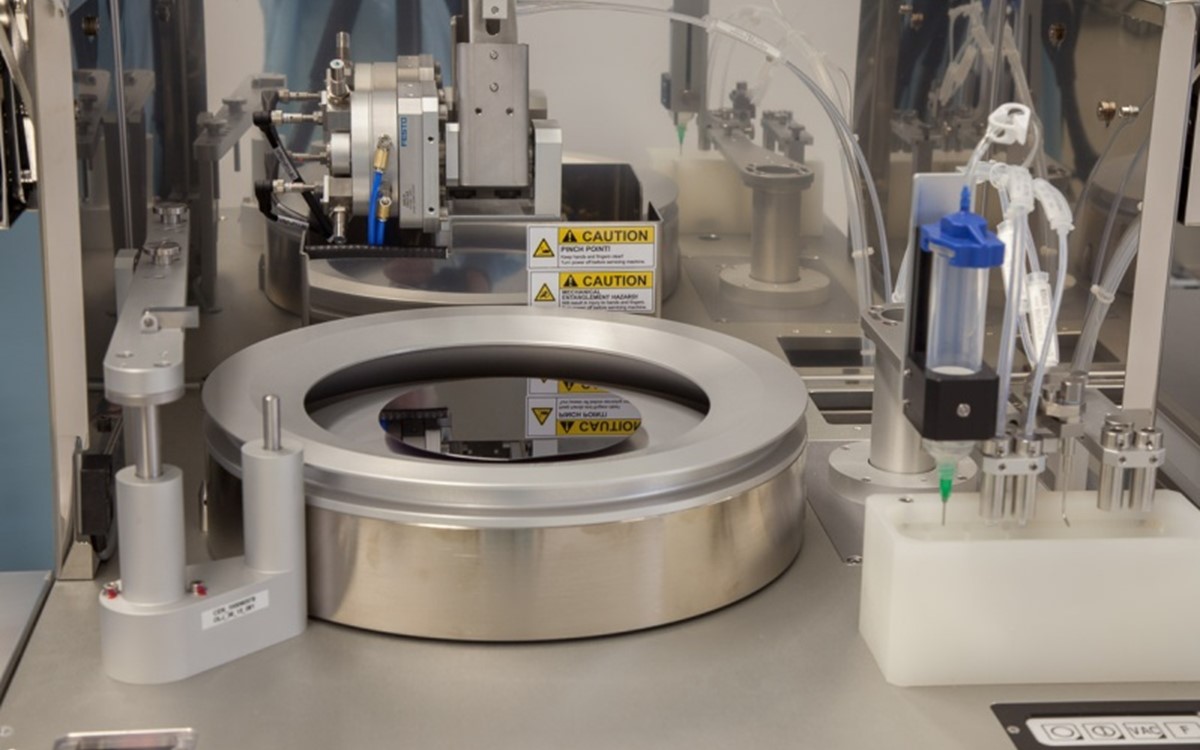
When it comes to semiconductor manufacturing, photoresist application is one of the most critical processes. This is something which can directly impact the precision and effectiveness of the photolithographic process, which is essential for creating intricate patterns on semiconductor wafers. It is difficult to underestimate the importance of following best practices for applying photoresists to make sure that high-quality patterns minimal defects and reliable performance of electronic devices can be assured. In this article, we provide a comprehensive breakdown of the best practices for applying focus photoresists and focus on the essential steps that are needed to achieve optimal results.

Best practices for applying photoresists
- Preparation
Photoresist application is an important step in semiconductor and PCB manufacturing as this is what affects the accuracy and quality of the photolithographic process. The process must begin with thorough preparation, including the cleaning of the substrate to remove any contaminants. This can include using solvents like acetone, isopropyl alcohol, IPA or specialised wafer cleaning solutions to ensure that the photoresist is able to adhere uniformly, and the resulting patterns are free from any defects. Heating the wafer then helps to remove moisture which also causes additional problems, whilst HMDS priming allows a layer of hexamethyldisilazane to be applied to promote the adhesion further. This is particularly crucial in certain types of photoresists and surfaces.
- Photoresist application
The photoresist application process usually includes a spin coating. During this stage, a drop of liquid photoresist is dispensed onto the centre of the wafer where it is spun at high speed to spread it evenly across the surface, forming a thin, uniform film. Adjusting the spin speed and duration can help control the thickness of the photoresist layer, as lower speeds result in thicker layers and higher speeds spread it much thinner.
During the photoresist application stage, it is vital to ensure that the photoresist solution is free of any air bubbles as these will cause defects in the pattern. This can be achieved by degassing the resist before application. This step can ensure that the coating is uniform, and the thickness is consistent across the entire substrate.
- Soft bake
There is then a soft bake, or prebake, stage which helps to stabilise the photoresist film and prevent issues like bubbling or peeling during exposure. This bake needs to be performed at a controlled temperature to ensure that solvent evaporation is even and the exact temperature and bake time will depend on the type of photoresist that has been used. Hotplates and ovens which have precise temperature controls are used to ensure even and uniform baking across the wafer.
- Exposure
During the exposure stage, the photoresist is exposed to UV light through a photo mask which contains the pattern that is due to be transferred to the photoresist. The photomask must be properly aligned with the wafer to ensure an accurate pattern transfer, and the UV exposure energy must be carefully controlled to ensure the resolution and development are correct.
- Post-exposure bake
A post-exposure bake can then take place to smooth out the photoresist edges and improve the overall resolution of the pattern whilst stabilising the chemical reaction that was initiated by the UV exposure. This stage usually requires a slightly lower temperature than the soft bake stage for a few minutes to help enhance the resolution of the pattern and improve the process window during development.
- Development
During the development phase, the unexposed areas of the photoresist are removed. It is important to check that the choice of developer, concentration and time is optimised to ensure the patterns are clean and accurate. Positive resist dissolves in the developer in exposed areas, whilst negative resist remain in the exposed areas and dissolves in the unexposed ones. It is important to precisely control the development time, as over- or under-developing the resist can lead to pattern distortion or incomplete transfer.
- Hard bake
There is then a hard bake which further hardens the remaining photoresists to improve its durability and resistance during the subsequent manufacturing processes. This hard bait needs to be conducted at a higher temperature to fully cure the resist and enhance its durability. There is a risk of over baking which can then cause the photoresist to flow or lose its pattern definition.
- Inspection and quality control
It is then important to inspect the substrate for any defects. Tickle microscopes or automated inspection systems can help to check for defects like particles, incomplete patterns or misalignments. It is also beneficial to make use of Critical Dimension (CD) Measurement, which can measure the critical dimensions of the pattern and ensure that they meet the design requirements.
- Storage and handling
It is essential that proper storage and handling of photoresist materials is conducted to maintain that effectiveness. They should always be kept in a cool, dark environment to maintain their chemical integrity. Any processed wafers should always be handled with extreme care to avoid contamination or damage to the photoresist pattern.
For semiconductor manufacturers to achieve high-resolution patterns with minimal defects, and unreliable device performance, it is essential that these best practices are always followed. This can help to ensure the success of the photolithographic process and therefore make sure that the quality of the final product is at its highest.
