Positive photoresist technology is central to the photolithography process. This is an important part of semiconductor manufacturing and microfabrication and allows for the creation of intricate microstructures of silicon wafers to produce highly complex integrated circuits and electronic devices. The positive photoresists define specific areas for etching or deposition on the substrate and so we will explore the positive photoresists process step by step and highlight its significance in the world of microfabrication.

Step one: Preparing the substrate
The first step of the positive photoresist process is to prepare the substrate, which is usually a silicon wafer. This wafer needs to be cleaned thoroughly to ensure that dust, oils and residues have been removed from the surface as they can interfere with the adhesion of the photoresist. This cleaning process uses a combination of chemical treatments to remove both organic and inorganic contaminants. Once it has been cleaned, the wafer is then dried through a heating process known as baking to eliminate any moisture on its surface. This step ensures that any subsequent application of the photoresist layer is uniform and will adhere properly.
Step 2: Applying the positive photoresist
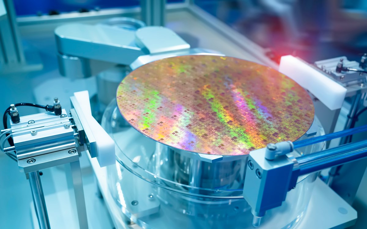
Once the substrate has been properly prepared, it is time for the positive photoresist to be applied. This is a light-sensitive polymer solution that is typically spun onto the wafer using a spin coating technique. During this process, the wafer is mounted onto a spinning platform and a small amount of liquid photoresist is deposited at its centre. The high-speed spinning of the wafer creates a centrifugal force which spreads the photoresist evenly across the surface to create a thin uniform film.
It is possible to control how thick the photoresist layer is by adjusting the speed of the spin and the viscosity of the resist. Thicker layers tend to be used for larger features, while thinner layers are more important for fine detail in high-resolution microfabrication.
Step 3: Soft bake
After the photoresist is applied, the wafer needs to undergo a process known as soft baking. During this process, the wafer is heated to a moderate temperature for a short duration to remove the solvents from the photoresist, improve its adhesion to the substrate, and make it less susceptible to damage during subsequent steps. This process is designed to harden the photoresist enough for exposure without causing it to lose its sensitivity to light. Soft baking will ensure that the resist can develop evenly and produce high-quality patterns.
Step 4: Exposure
During the exposure step, a photomask which contains the desired pattern of the microstructures is placed over the wafer. This acts a bit like a stencil, allowing light to pass through specific areas while blocking others. When the wafer is exposed to UV light, the light-sensitive areas of the positive photoresist go through a chemical change which makes them more soluble in the developer solution that will be used in Step 5. The areas that are exposed to light will be removed during development and the unexposed areas will be left behind to form the desired pattern on the wafer.
Step 5: Development
Once the exposure is completed then the wafer needs to be immersed in a developer solution which will selectively dissolve the exposed areas of the photoresist. This helps to create the patterned photoresist layer which then acts as a mask during etching or deposition. The developer solution needs to be carefully chosen to ensure that only the exposed regions are dissolved. Once the development is complete, the wafer should be rinsed to remove any remaining developer solution and unwanted photoresist particles. This ensures that a clean, precise pattern remains, matching the design on the photomask.
Step 6: Hard bake
Once development is complete, the wafer needs to be subjected to hard baking at a high temperature. This solidifies the remaining photoresist to enhance its resistance to the chemicals used during etching or deposition. The hard bake can improve the durability of the photoresist to keep it intact during the next steps of the fabrication process.
Step 7: Etching or deposition
During the etching process, the exposed regions of the substrate are removed using a chemical or plasma etchant, which creates the final microstructure. For deposition, materials such as metal or dielectric layers are added to the exposed regions of the wafer. The photoresist layer protects the areas that should not be etched or deposited to ensure the creation of precise and controlled structures on the wafer.
Step 8: Photoresist removal
Once the etching or deposition is complete, the remaining photoresist is no longer needed and should be removed. This requires a photoresist stripping process where solvents or plasma are used to lift off the hardened resist to leave behind only the patterned microstructures on the substrate.
The significance of positive photoresist technology
When microelectronic devices are being produced, then positive photoresist technology becomes an essential tool to enable the creation of intricate and highly accurate patterns on silicon wafers. They offer high precision and resolution, which are essential for developing the smaller and more powerful electronic devices that are now in high demand. Positive photoresists offer a versatile and scalable process to make it suitable for a wide range of microfabrication applications. This means it can be used in a wide number of industries, from consumer electronics to telecommunications, automotive technology and even aerospace.
The positive photoresist process is a cornerstone of photolithography, which enables the creation of highly detailed microstructures for modern semiconductor manufacturing. By understanding the process behind the use of positive photoresists, engineers can design and fabricate complex integrated circuits that offer high levels of precision and enable them to drive innovation in new and exciting ways.
