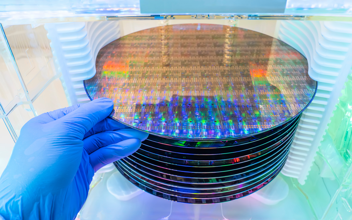
Every year, semiconductor manufacturers push the limits of what’s possible – smaller geometries, greater efficiency, and faster processing speeds. Yet behind every technological leap lies a quieter transformation in materials.

From next-generation photoresists to new metallisation techniques and sustainable chemistries, the materials that underpin semiconductor manufacturing are evolving rapidly. To stay competitive, understanding these changes and partnering with the right suppliers is essential.
At A-Gas Electronic Materials, we work alongside fabs and research institutions across the UK, Ireland, Europe and beyond to deliver semiconductor material solutions that enable these advancements. Here’s a look at the key innovations shaping 2025 and beyond, and how flexible sourcing helps manufacturers adopt them effectively.
- The next generation of photoresists
As lithography continues to advance, so too does the need for higher-performance photoresists. For extreme ultraviolet (EUV) and high-NA lithography, materials are being engineered to achieve greater sensitivity, improved line-edge control, and enhanced etch resistance, all while maintaining low defectivity. Negative-tone and hybrid resists are gaining traction for their superior pattern fidelity, while inorganic resists such as HSQ and SML are enabling patterning at sub-10 nm nodes.
Through our partnerships with EM Resist and other leading manufacturers, we supply and support a broad range of photoresists and ancillaries tailored to these emerging requirements. Our technical specialists help customers qualify and integrate the right products for their processes, whether that’s EUV, DUV, or e-beam applications, ensuring consistent performance as lithography technologies evolve.
- Advanced metallisation and interconnect materials
Copper has been the backbone of semiconductor interconnects, but as feature sizes shrink, new materials are taking the spotlight.
Cobalt and ruthenium are increasingly used to improve electromigration resistance and reduce line resistance at smaller geometries. These materials also offer advantages for next-generation interconnect architectures, such as barrier-less metallisation and hybrid bonding.
A-Gas EM’s metallisation technologies portfolio provides access to specialist plating chemistries, surface treatments, and adhesion promoters developed for advanced interconnect and packaging applications. By working with multiple suppliers, we help customers evaluate alternatives quickly, giving flexibility to qualify new metals and chemistries without production delays or supply-chain disruption.
This approach means engineers can test and transition to next-generation materials confidently, supported by our local stockholding and responsive technical service.
- Materials enabling wide-bandgap power devices
The demand for efficient power electronics is fuelling rapid growth in SiC and GaN technologies. These wide-bandgap materials operate at higher voltages and temperatures than conventional silicon, delivering greater energy efficiency and power density, essential for electric vehicles, renewable energy systems, and data-centre infrastructure.
Manufacturing these devices introduces new material challenges, from wafer cleaning and surface preparation to metallisation and encapsulation. We supply photoresists, etchants, cleaning chemistries, and metallisation materials compatible with SiC and GaN processes, helping streamline qualification and achieve consistent yields.
By partnering with multiple manufacturers, we ensure customers can access the most suitable formulations for their specific device architectures, while maintaining continuity of supply as demand for compound semiconductors accelerates.
- Advanced packaging and interconnect integration
While front-end innovation captures headlines, the real race for performance and efficiency is increasingly happening at the packaging level.
Technologies such as fan-out wafer-level packaging, 2.5D/3D stacking and chiplet integration require a new generation of materials, from fine-line plating chemistries to underfills, adhesives, and cleaning solutions optimised for micro-scale features.
Our metallisation and ancillary portfolios are already supporting customers active in advanced packaging and interconnect integration. Our flexible sourcing model allows us to bring together materials from multiple suppliers, enabling customers to qualify entire process chains with the confidence that each component is optimised for compatibility and performance.
- Sustainability and circularity in semiconductor materials
Sustainability is no longer a secondary consideration; it’s a core part of the decision-making process for the whole supply chain. Across the industry, R&D is focused on reducing volatile organic compounds, re-formulating chemistries for lower waste, and improving container re-use and recycling. A-Gas EM’s own environmental initiatives align closely with this direction – our group-wide circular economy model prioritises responsible chemical lifecycle management, recovery and reuse wherever possible.
We actively collaborate with manufacturers developing low-impact solvents and eco-optimised process materials, ensuring customers can achieve both performance and environmental goals. Sustainability is no longer about compliance – it’s a measurable performance metric that forward-thinking businesses are building into their strategies.
- The power of flexible sourcing
The pace of material innovation creates opportunity, but also complexity. A single-source model can limit how quickly you can respond to new technology requirements or qualify alternative materials.
By contrast, flexible sourcing through A-Gas EM provides direct access to multiple world-class manufacturers, supported by our in-house technical knowledge. This enables customers to evaluate new materials efficiently, reduce risk through multi-supplier resistance, and maintain control over process optimisation.
We bridge the gap between global innovation and local implementation, simplifying supply chains while preserving agility. Whether supporting a pilot line or a high-volume production environment, our team ensures that materials integration, logistics, and technical service all work seamlessly together.
Looking ahead, the semiconductor materials landscape will continue to evolve rapidly. The convergence of AI compute, automotive electrification, and 5G/6G infrastructure will demand new generations of resists, dielectrics, metallisation chemistries, and packaging solutions.
Success will depend on collaboration. At A-Gas EM, we combine technical expertise, trusted supplier networks, and responsive local support to help our customers do exactly that. By offering flexibility instead of limitation, and partnership instead of pure supply, we enable manufacturers to focus on innovation, confident that their materials strategy is ready for whatever comes next.
For further semiconductor materials insights, get in touch with our technical team today.
