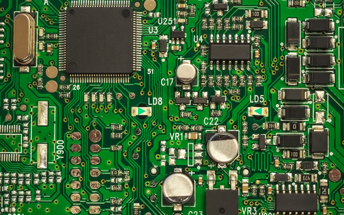
Printed circuit boards (PCBs) are at the heart of every modern electronic device. But running a high-volume PCB line isn’t without challenges. Small deviations in chemistry, process control, or material quality can quickly snowball into downtime, costly scrap, and missed deadlines.

At A-Gas EM, we’ve spent decades helping manufacturers across the UK and Ireland get their lines running smoothly and keep them that way. From sourcing world-class materials to providing on-site technical support, we’re here to help you tackle the most common PCB line issues head-on.
Here’s a closer look at the most common PCB line issues, and how targeted solutions can keep PCB production stable and predictable.
Imaging and soldermask – getting the base right
The imaging stage sets the tone for the entire build. If your dry film photoresist doesn’t adhere evenly, or if liquid soldermask has pinholes or poor coverage, the entire board’s performance is at risk.
A high-quality dry film photoresist is essential here, providing strong adhesion and fine-line resolution. Issues such as resist lift-off, under-developed areas, or uneven coating often come down to surface contamination, variations in lamination temperature or pressure, or developer chemistry drifting out of specification.
Choosing a stable, high-performance dry film photoresist, matched to your process conditions, can make a significant difference. Paired with the right developing solution, it produces clean results that stand up to downstream processes. And when it’s time for removal, precise dry film photoresist stripping clears the surface without damaging the copper, ready for plating or soldermask application.
For liquid soldermask, levelling, curing, and adhesion are equally critical. Variations in viscosity, inadequate pre-cleaning, or under-curing can all lead to rework or failures. Industry best practice recommends controlling material viscosity within manufacturer guidelines, ensuring complete surface preparation, and following curing profiles precisely to achieve durable, defect-free coverage.
Metallisation and plating – building reliable layers
Once the image is fixed, metallisation creates the conductive pathways and through-hole connections that define the board’s electrical performance.
Electroless copper is the foundation of this stage, depositing an even, conductive layer over drilled hole walls and panel surfaces. Incomplete coverage or poor adhesion often results from contamination, poor surface preparation, or chemistry that has drifted outside its control limits.
Using a reliable electroless copper chemistry, supported by routine bath analysis, helps maintain deposit uniformity and adhesion. Further plating steps, such as acid copper plating, tin plating, or electrolytic nickel and gold plating, require careful control over current density, agitation, and anode condition to produce bright, even finishes.
For high-reliability boards, ENIG plating (electroless nickel, immersion gold) provides an excellent solderable surface with flat topography for fine-pitch assembly. Success with ENIG depends on maintaining nickel bath stability, controlling gold porosity, and ensuring thorough rinsing to avoid defects such as black pad.
Finishing – protecting performance and appearance
The final finish protects the board’s solderability and corrosion resistance. It also provides the visual quality customers expect.
ENIG remains a leading choice, delivering a long shelf life and flat, solderable surfaces for fine-pitch components. Alternatives include ENEPIG, ASIG (Autocatalytic Silver with Immersion Gold), OSP and immersion tin, which also deliver strong performance when process control is tight.
Whatever the chosen finish, stability and cleanliness are critical. Bath contamination, poor rinse water quality, or handling errors can all undermine final quality. In each case, the right chemistry and maintenance routines prevent defects and preserve long-term reliability.
Maintaining control across the line
Every PCB line has its own challenges, shaped by its equipment and operator routines. The difference between constant firefighting and smooth, predictable production often comes down to process stability and support.
Working with a specialist PCB distributor gives manufacturers access to high-performance chemistries, process expertise, and responsive supply. It’s a partnership that helps identify root causes, maintain control, and ensure every stage of the line delivers the results it should.
At A-Gas EM, we combine:
- High-performance chemistries – from dry film photoresist and liquid soldermask to ENIG, ENEPIG, ASIG, OSP and Immersion Tin systems.
- Technical process support – on-site troubleshooting, analysis, and operator training.
- ISO-certified laboratory testing – accurate, fast chemical analysis to maintain process control.
- Sustainable supply – UK warehousing for fast delivery, reducing your environmental footprint.
We’re here to keep your PCB line producing high yields, consistently and reliably. If you’re seeing yield drops, plating defects, or finish problems, get in touch with us.
Our technical sales team can help diagnose the root cause and recommend the right chemistry and process changes to fix it.
