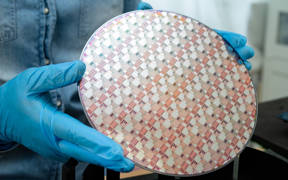
Semiconductor manufacturing is a complex and intricate process where photolithography is critical when it comes to defining the patterns that form the circuits on a microchip. At the heart of all of this is the photoresist, of which there are two main types: positive and negative photoresists. The positive photoresists are widely used thanks to their high resolution and precise patterning capabilities, so, in this article, we explore their role in semiconductor manufacturing by looking at their working principles, advantages and their significance in creating intricate semiconductor patterns.

What are positive photoresists?
A positive photoresist is a light sensitive material that is subject to a chemical transformation when it is exposed to ultraviolet (UV) light. During this process, the areas which are exposed to light become more soluble in a developer solution which allows them to be removed, keeping the unexposed areas intact. This is all designed to enable the formation of the fine patterns that are needed for fabricating semiconductor devices.
Typically, photoresists are made-up of three components. The first is the photoactive compound (PAC) which undergoes a chemical reaction when exposed to UV light to alter its solubility, whilst resin provides the necessary mechanical strength and adhesion to the substrate. The third component is solvent, which will help to apply the photoresist as a uniform thin film on the semiconductor wafer.
How do positive photoresists work?
The process of photolithography using positive photoresists involves several different steps which are each crucial to ensuring the high precision patterning that is needed. To start with, a silicon wafer is coated with a thin, uniform layer of positive photoresist through a process called spin coating. This coated wafer is then heated during a soft bake process to remove any excess solvent and improve the adhesion. During the exposure stage, a mask containing the desired pattern is placed over the wafer and a UV light is shone onto it. The exposed areas of the photoresists then undergo a chemical transformation to increase their solubility.
Once this has been done, the wafer is then immersed into a developer solution to dissolve the exposed areas and leave behind a patterned resist layer which acts as a stencil for subsequent processes such as etching or material deposition. After the desired pattern has been transferred onto the wafer, the remaining photoresist is then stripped away to reveal the final circuit structure.
The advantages of positive photoresists
Positive photoresists are preferred in semiconductor manufacturing since they allow for extremely fine feature sizes that are essential for modern semiconductor devices. This high resolution also helps to create well-defined patterns that can ensure precise circuit designs. Positive photoresists are also preferred due to their predictable solubility behaviour and ease of development, which all contribute to consistent manufacturing outcomes. Positive photoresists tend to work well with deep ultraviolet (DUV) and extreme ultraviolet (EUV) lithography to help enable next-generation chip fabrication.
Applications in semiconductor manufacturing
Positive photoresists have several different uses, and they are instrumental in integrated circuits (ICs) by helping to create intricate layers of transistors and interconnects in microprocessors and memory chips. They are also a significant part of the production of Microelectromechanical Systems (MEMS) as they can be used to fabricate small mechanical structures such as sensors and actuators. Positive photoresists also play a role in the development of wafer-level packaging and 3D integration technologies.
Future developments in positive photoresists
Semiconductor technology is continuing to advance, which means that there is an increasing need for photoresists, which are capable of supporting even smaller feature sizes and higher performance demands. This is why researchers are now working on novel materials and formulations, including chemically amplified resists (CARs) and metal-organic resists to enhance resolution and efficiency. There are also some improvements in EUV lithography, which are driving the development of new positive photoresists capable of withstanding higher energy exposure while still maintaining their pattern fidelity.
There is no doubt that positive photoresists have become a fundamental component of semiconductor manufacturing, as they enable the creation of highly detailed and precise circuit patterns. The combination of their high resolution, excellent pattern fidelity and compatibility with advanced lithographic techniques makes them indispensable in the production of microchips. It is therefore clear that as the semiconductor industry continues to move towards smaller and more powerful devices, the ongoing evolution of positive photoresists will continue to shape the future of electronics and computing.
