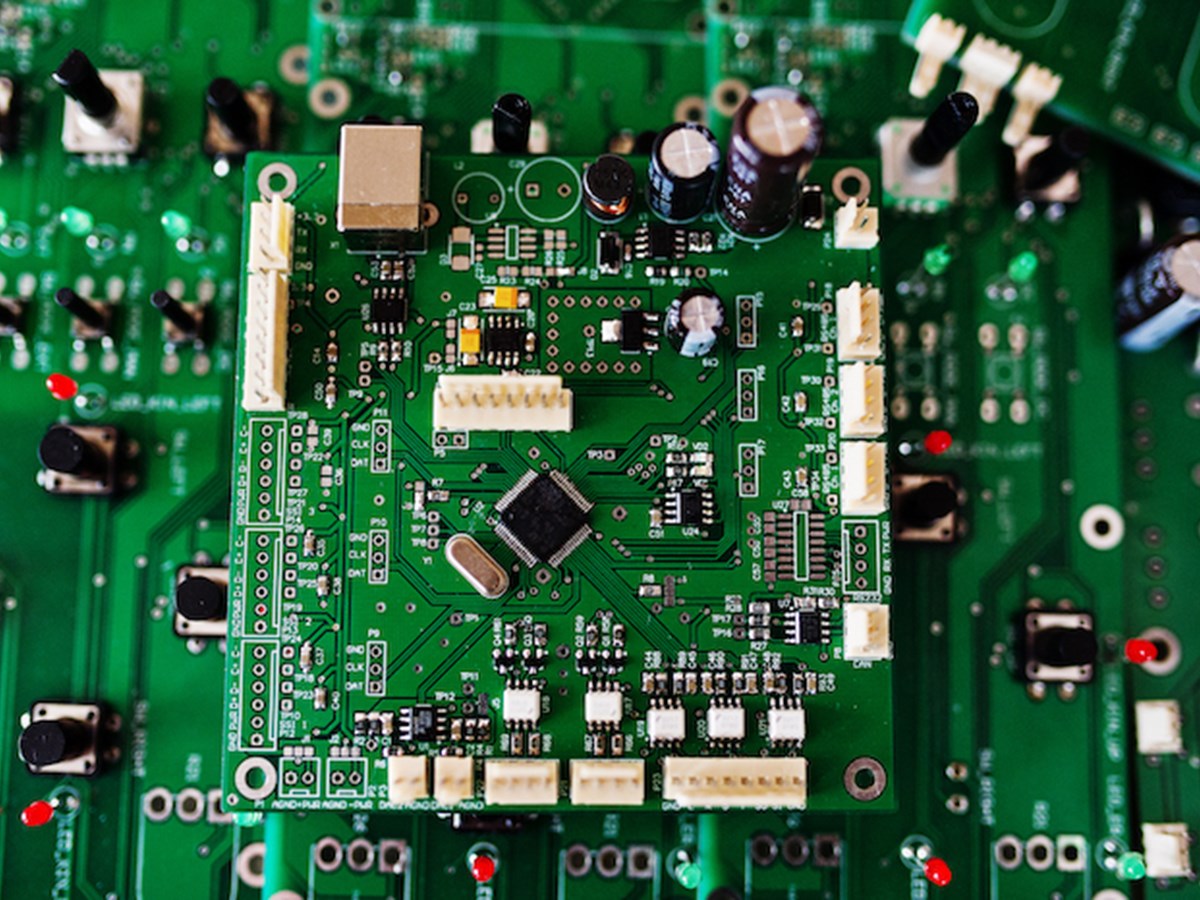
A key innovation in printed circuit board manufacturing has been Liquid Photoimageable Soldermask (LPI). This offers precise and reliable protection for electronic circuits to improve the overall quality and performance of the PCBs. Technology has advanced and so the methods to apply and enhance these soldermasks have had to keep up, and LPI is now the preferred choice thanks to the huge number of benefits it can provide. In this article, we explore the advancement and advantages of LPI and outline the best practices for applying photoresists in semiconductor manufacturing to ensure optimal results and high-quality outcomes.

What is a Liquid Photoimageable Soldermask (LPI)?
Liquid Photoimageable Soldermask (LPI) is a liquid coating that is applied to the surface of a printed circuit board (PCB) to protect any copper traces from oxidation, corrosion, and accidental solder bridging during the soldering process. What makes it special is its ability to be selectively hard by using UV light. The provision of selective curing allows for high precision in circuit board protection.
Advancements in LPI technology
There have been several advancements in LPI technology in recent years which have made it more adaptable to the ever-changing needs of the electronics industry. It now allows for finer and more detailed resolution, making it suitable for high-density interconnect boards as well as more complex circuit designs. This has been very important when it comes to supporting the growing trend of miniaturisation in electronic devices.
Moisture, heat and chemicals can all be damaging to the lifespan of a PCB, and so modern LPI formulations have been developed to offer increase resistance to these environmental factors. This is especially important in harsh environments such as the automotive, aerospace and industrial sectors.
It has also been important to ensure that new LPI products focus on sustainability so they now feature reduced volatile organic compounds (VOCs) which are less harmful to the environment. These eco-friendly options mean that manufacturers can reduce their environmental impact while still meeting any necessary regulatory requirements.
We live in a world that moves at great speed, and PCB manufacturing is no exception. It has therefore been necessary to harness UV light technology to reduce the curing times for LPI which can then lead to shorter production cycles.
Benefits of LPI in PCB manufacturing
One of the main benefits of LPI is the levels of precision and accuracy that it can offer. The photoimageable properties mean that there can be highly accurate application processes, ensuring that only the desired areas of the PCB are protected. This can help to reduce errors and defects and can ensure that PCBs perform better.
As LPI coatings also provide excellent protection against physical damage such as scratches and abrasions, they can enhance the reliability and longevity of any circuit board. There is also a need for finer pitch components as electronic devices continue to become smaller. LPI's ability to conform to intricate designs means that it is ideal for this kind of electronic manufacturing.
Whilst it may be the case that the initial cost of introducing LPI is higher than some other methods, the precision that it offers means that waste and rework are reduced significantly to lower the ultimate cost of manufacturing.
Best practices for applying photoresists
Photoresist application is an important step in semiconductor and PCB manufacturing as this is what affects the accuracy and quality of the photolithographic process. The process must begin with thorough preparation, including the cleaning of the substrate to remove any contaminants. This will ensure that the photoresist is able to adhere uniformly and that the resulting patterns are free from any defects. The photoresist application process includes spin coating, spray coating, and curtain coating, depending on the specific requirements of the process. These can ensure that the coating is uniform, and the thickness is consistent across the entire substrate.
There is then a soft bake, or prebake, stage which helps to stabilise the photoresist film and prevent issues like bubbling or peeling during exposure. This bake needs to be performed at a controlled temperature to ensure that solvent evaporation is even.
During the exposure stage, UV light is used to harden the photoresist in areas where it will remain. This alignment and exposure must be carefully controlled to ensure that the patterns remain sharp and accurate. A post-exposure bake can then take place to smooth out the photoresist edges and improve the overall resolution of the pattern whilst stabilising the chemical reaction that was initiated by the UV exposure.
During the development phase, the unexposed areas of the photoresist are removed. It is important to check that the choice of developer, concentration and time is optimised to ensure the patterns are clean and accurate. There is then a hard bake which further hardens the remaining photoresists to improve its durability and resistance during the subsequent manufacturing processes.
It is then important to inspect the substrate for any defects, whilst high-resolution imaging and automated inspection tools can ensure the photoresist application meets all quality standards. It is essential that proper storage and handling of photoresist materials is conducted to maintain that effectiveness. They should always be kept in a cool, dark environment to prevent any premature degradation.
Liquid Photoimageable Soldermask has revolutionised PCB manufacturing thanks to its precision, durability and sustainability. When coupled with the best practises in photoresist application, LPI can ensure a high quality, reliable and cost-effective production process.
