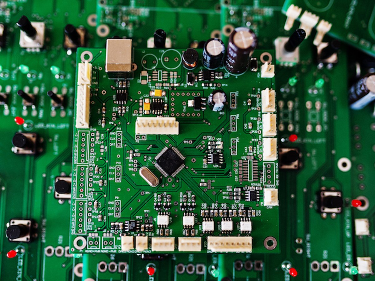
Semiconductors form the basis of almost any modern electronic device. As the desire to make these devices smaller, faster and more efficient continues, the manufacturing processes involved have had to adapt. Here, we look at some of the most significant innovations in the semiconductor manufacturing processes in recent years.

Extreme Ultraviolet (EUV) Lithography
Many manufacturers have been used to using Deep Ultraviolet (DUV) lithography, but they are now making the switch to Extreme Ultraviolet (EUV) lithography. This EUV lithography has proved to be a significant innovation in semiconductor manufacturing processes as it uses light with a wavelength of 13.5 nanometers compared to the 193 nanometers needed for DUV. This means semiconductor wafers can now have much smaller features and chips with higher transistor densities can be created. EUV lithography can be a high-cost and complex option at the moment, but it is gradually being adopted by more and more semiconductor companies who are aiming to stay competitive in a market that is moving continuously.
3D chip stacking and advanced packaging
There may be a modern desire to make everything smaller but achieving it can sometimes be a different matter. To try and meet this demand, the semiconductor industry is now using 3D chip stacking and advanced packaging techniques. This provides a way of increasing transistor density without shrinking the individual transistors themselves by vertically integrating multiple layers of circuits within a single chip package to increase performance by reducing the distance that data needs to travel and enabling more efficient use of space. The advanced packaging techniques such as chiplet design and silicon vias (TSVs) make this even more effective. When it comes to the development of high-performance computing applications, artificial intelligence processes and other demanding technologies, these innovations have proved to be essential for achieving power, efficiency and performance.
Quantum computing materials and processes
Quantum computers are creating a new realm of computing power. They require qubits which can represent multiple states simultaneously. Materials such as superconductors, topological insulators and diamond-based nitrogen-vacancy centres are now being used to create these stable and reliable qubits. There are also new manufacturing processes being developed to handle the very precise fabrication that is needed for these quantum devices and so techniques such as atomic layer deposition (ALD) and molecular beam epitaxy (MBE) are being refined to build the nano structures that cubit formation requires.
Advanced semiconductor materials
Silicon was once an essential ingredient for all semiconductor devices, but to help enhance their performance, many chips manufacturers are now turning to materials such as gallium nitride (GaN), silicon carbide (SiC) and indium gallium arsenide (InGaAs). This is because they boast superior electrical properties. GaN and SiC have been found to be best suited to power electronics as they are capable of operating at high voltages, frequencies and temperatures, therefore making them most suitable for electric vehicles, renewable energy and telecommunications.
Al and machine learning in manufacturing
Artificial intelligence (AI) and machine learning (ML) are playing increasing roles in our everyday lives, so it stands to reason that they should also transform the semiconductor manufacturing world. As these technologies can analyse vast amounts of data from manufacturing equipment, identifying patterns and predicting potential issues, they can reduce downtime and improve yields, making production not only more efficient but also more cost-effective.
AI and ML are also a big factor in design automation as they can help engineers create more complex chip architectures. They have been put to use automating routine tasks and optimising design parameters to enable faster innovation and reduce the time it takes for new semiconductor products to hit the market.
Sustainable manufacturing practices
There is no doubt that all manufacturers now need to be aware of their environmental impact on the planet. To reduce energy use, minimise waste and recycle materials during production processes, many businesses are now developing energy-efficient manufacturing equipment and making use of renewable energy sources. There are also several advancements when it comes to issues of water purification and recycling technologies to further reduce the environmental footprint of semiconductor fabrication.
Technology is a fast-moving landscape and every element within that needs to work hard to keep up. The semiconductor manufacturing process is constantly innovating to help produce devices that are not only faster and smaller but also more powerful and reliable. They are embracing new forms of technology whilst also keeping an eye on their environmental impact to make sure they can strike a balance between technological progress and environmental responsibility.
Harness the power of cutting-edge manufacturing innovations like EUV lithography, advanced packaging, and AI-driven processes to enhance your production capabilities.
Contact us today to learn how our expertise and solutions can help you drive efficiency, sustainability, and performance in your semiconductor manufacturing operations.
