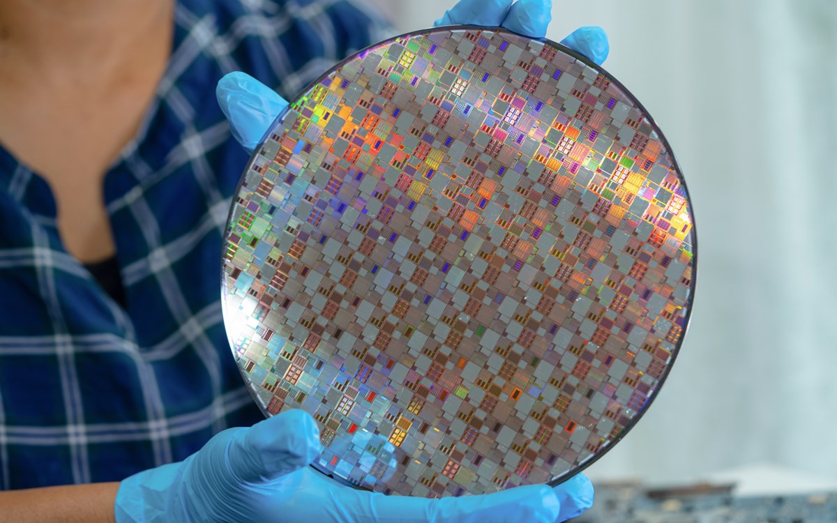
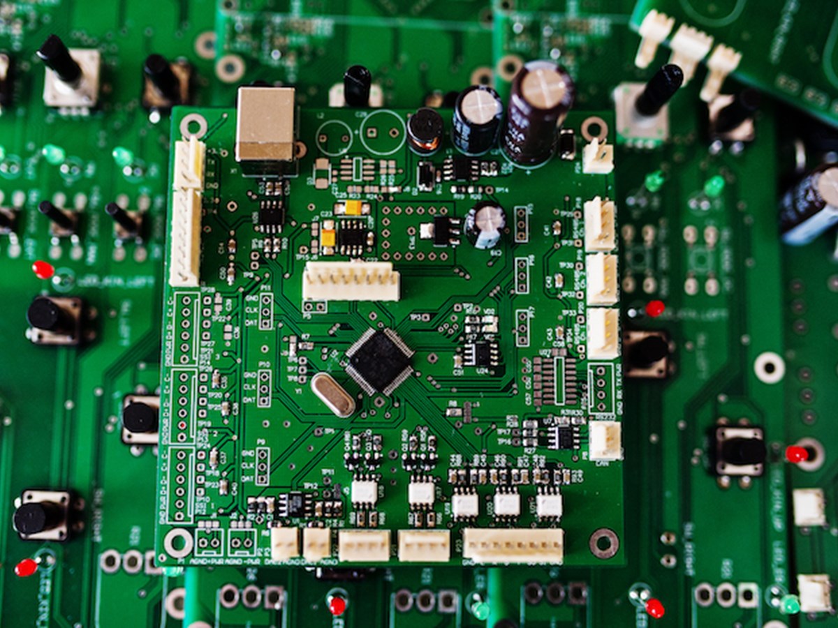
As modern technology evolves, so do the techniques behind it when it comes to producing microchips and integrated circuits. These are central to the way in which our smartphones and supercomputers work, and photolithography is an important technique used as part of semiconductor fabrication. This requires the use of positive photoresists, which use light to trigger chemical changes that can help to provide the pattern for any etching or depositing of materials on the circuit of a semiconductor device. This is a very specialised technique and so we thought this was a great opportunity to answer some of the most frequently asked questions when it comes to the subject of positive photoresists.

What is a positive photoresist?
Positive photoresists are light-sensitive materials used in the photolithography process. They are made up of resins, photoactive compounds and solvents to create a pattern that can be used as a template on a semiconductor wafer. This template is used for etching or depositing materials on the wafer to form intricate circuits within a semiconductor device.
How do positive photoresists work?
To begin with, a thin layer of photoresist is applied to a semiconductor wafer, which then needs to be baked to remove the solvent and leave behind a solid, uniform film. It is then exposed to ultraviolet light through a photomask, which has the circuit patterns etched onto it. As UV light passes through the photomask, it can interact with the photoresist in the exposed regions. A chemical reaction then takes place, ensuring that the exposed areas of the photoresist become soluble in a developer solution. This developer removes any exposed regions of the photoresist, which leaves behind a pattern identical to the one on the photomask. It is this pattern which then becomes the etching template.
Why is it called a positive photoresist?
These types of photoresists are described as positive, due to the fact that the exposed areas become more soluble in the developer solution so that they can be removed. If the area is insoluble and remains on the substrate, then it is known as a negative photoresist.
Why are positive photoresists used?
One of the greatest advantages of a positive photoresist is the level of accuracy that it can offer. Thanks to their ability to work with smaller features and well-defined edges, they can create very intricate circuit patterns. These allow for better performance of the device in question and greater levels of reliability. Without this level of high resolution and detail, there may be defects or inaccuracies in the photoresist pattern. This can then be responsible for issues such as electrical shorts, poor connectivity, or decreased device performance. Positive photoresists have also been found to have better thermal stability than negative photoresists.
Why choose a positive photoresist instead of a negative one?
Choosing between positive and negative photoresists will depend on the requirements of each semiconductor manufacturing process. Positive photoresists tend to be chosen when high resolution and fine patterning are essential whilst negative photoresists tend to be preferred in applications that have thicker resist layers or greater etch resistance.
What are the limitations of positive photoresists?
The increased accuracy and performance of a positive photoresist can mean that it is a more expensive process. In addition to this, it may also require more precise control throughout the photolithography process to ensure that high levels of accuracy are maintained. As positive photoresists are sensitive to certain wavelengths of light, this can sometimes limit their compatibility with photolithography systems, and so they may not always be the most suitable option.
The semiconductor industry is developing at a rapid rate and positive photoresists are playing a central role in this. Their ability to provide high resolution and accurate pattern transfer means that precise patterning can now be used with ease when it comes to producing modern integrated circuits, and so it is likely that their use will continue to grow as consumers demand even smaller, faster and more efficient devices.
Discover the power of positive photoresists for creating high-resolution, intricate circuit patterns that drive the performance of today’s advanced devices.
Contact our experts now to learn how our cutting-edge photoresist solutions can enhance your production process and help you meet the demands of an ever-evolving market.
